8x8x8 RGB LED Cube - Part One
April 04, 2021
I originally made an LED cube about 6 years ago following this tutorial on Instructables. I ordered the PCBs from the author, ordered the parts needed from Mouser and eBay, and spend 3 days over the weekend building the whole thing out. At the time, it was exiting to build and have this working, but I wanted to make one better. It was good practice, but eventually I knew I would want to make an RGB version. I just needed to find the time.
When looking for things to do during the Covid quarantine, I remembered wanting to build an RGB cube and got to researching. This tutorial seemed to be the most complete resource for building out the cube, but I wanted to understand how it works instead of just assemble a kit. Besides, I wanted to kill some time and once I started I was determined to see it through.
Cube Construction
RGB LEDs mainly come in two varieties: common anode (+) and common cathode (-). Being the one unit is essentially made up of three separate diodes of each color, you don’t want there to be an anode and cathode for each color, so you can combine all the anodes or cathodes.
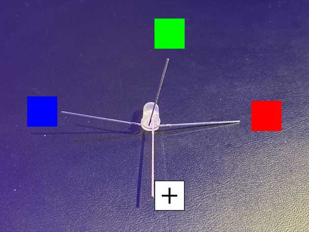
We need to use common anode LEDs, as we will see why later. All 512 LEDs need to be bent like Figure 1.
There seems to be two ways to construct the layers. The first way is to lay out templates for an entire layer properly spaced on your work surface, and solder all the support wires together. The second way is to make all the pillars first, then combine each into a layer.
Constructing each pillar first and then attaching them seemed to be the less error prone approach to me, as you don’t need to tape each template piece at the appropriate spacing. The 3D models for the method I used from the original cube are located on Thingiverse. The pillar method only really needs the stand_8.stl, but I also ordered the stand_888_25_b.stl as it made spacing the pillars into the layers easier. The first model has spacing holes as well, but it’s a bit clunkier to use for that purpose. I had the models 3D printed at Sculpteo, my first set I had printed with SLS (Plastic), Nylon PA12 100-120µ (White). I had a later round made with Multijet Fusion, PA12 (Grey). The SLS templates are actually the only ones I used to construct my cubes, but compared to the Multijet models, the LEDs slid into the template easier with the Multijet, whereas the SLS model was a bit tighter, and might make your first couple pillars a millimeter out or so spacing wise until it’s worn in.
The LED leads are too long to fit into the template, so I cut each of them about halfway before inserting into the templates to solder. I didn’t worry about accuracy here, as I would cut them again after soldering the vertical wires.
When you have all 8 LEDs into the template for a pillar, you now solder a wire for each of the cathodes all the way down. For my original cube, I unravelled silver colored copper wire, 22 AWG, meant for jewelry that I got on Amazon. I measured and cut to 25cm lengths. It’s key that you straighten the lengths, and the easiest way I found, and you eventually get really fast at it, is to grab both ends of the wire with identical pliers and pull. You get a nice satisfying stretch in the wire, and it becomes perfectly straight. Make sure you wear gloves of some kind, or you will start to get blisters. You need at least 272 lengths, but make a few extra as you will probably ruin a few. 25cm is a bit longer than needed, but I was scared to go shorter in case I needed the extra length, I didn’t want to cut it close, but you could get away with 23cm. You cut off all but 2.5cm from the bottom after it’s soldered onto the PCB.
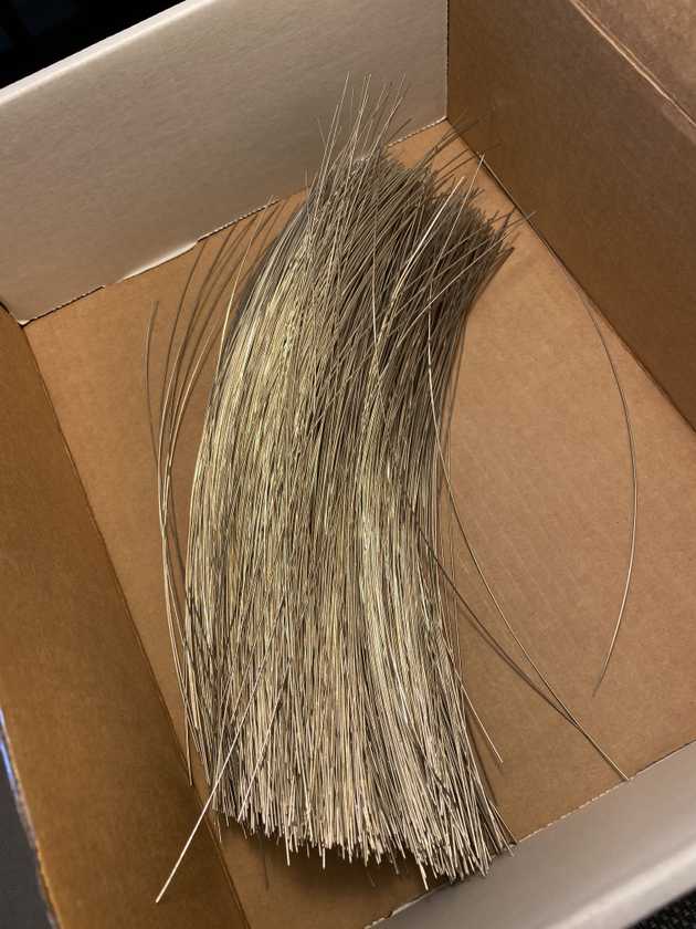
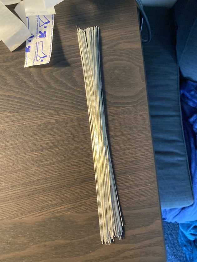
For my second cube, cutting the wire was my least favorite part, I found the spooled wire harder to work with before straightening as it wanted to maintain it’s coils from being spooled. I got Remington Industries in Illinois to cut me lengths of 25cm, but looking back now it probably wasn’t worth it, I would just buy a spool of their 22 AWG tinned copper wire from their eBay store or website. I still had to straighten the wire by hand. Working with this wire was much more pleasant, it soldered easier and seemed much higher in quality.
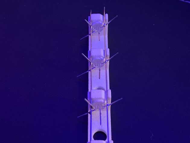
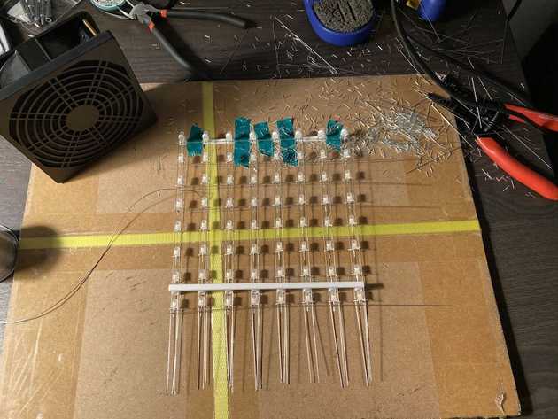
In Figure 4, the wires are all placed on the left of each of the LED leads and soldered in place. Try to make sure the leads and the wire are touching on their own without having to rely on the solder to bring the two together.
It’s imperative to test each of the LEDs before each layer is created, but I found failures with the LEDs I used to be rare, in fact, I had none on any of the LEDs I used. So instead of testing all the LEDs at this point, I decided to test them after soldering each of the columns. If one happened to fail. I would have to throw out the whole column likely, but it saved enough time I thought the tradeoff was worth it. After the pillar is tested, you can cut off the excess wire for each of the LED leads.
You can either solder 64 pillars at once and construct all the layers after, or solder 8 pillars and construct each layer right after.
I used the two secondary 3D printed pieces to space out the layers, and used some tape to hold them in place so they didn’t shift while working on them. The layers have their “flat side” up and slanted slightly to the left, they should be able to lay on their side in this position. Make sure your pillars aren’t tilted/scewed, otherwise your layer will not be square when the anodes are soldered together for each row.
Every row of LEDs needs a wire soldered across all the anodes in the row, through the middle of the leads. After this is complete you can cut off the excess.
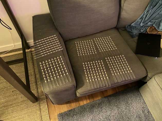
When you have a layer complete, the most frustrating part is inserting all the leads into each of the holes on the PCB base. I found it was easier to ensure that each pillar had all their leads the same length, so trim them to the shortest lead for each pillar in the layer. I found that positioning the PCB between my knees, and starting from one side, insert all the leads, and slowly move to the other side until all the leads are insterted.
When that’s complete, you can use the 3D printed template you soldered the pillars with as a spacer on the bottom of the PCB so the first LED slot to measure how high off the PCB the layer should be positiond. Once you have a side at the right height, bend a lead, and do the same on the other side. This will hold the layer at the correct height needed.
Now you have to carefully ensure that the layer is completely vertical, I usually found this easier by hanging the layer off the edge of my desk, and then moving the layer to be vertical, and being really carefule, solder a lead on each side and that should lock it into place. Make sure it’s positioned perfectly at this point. Once it is, solder all the leads.
After the whole layer is soldered to the PCB, you can clip all the leads on the underside. Now you should plug the cube in and test it, because if there are any issues, finding out after you’ve soldered all the layers will be near impossible to fix if the broken layer is behind others.
Each LED column has a hole in the PCB for an anode, where from back-to-front the anodes are for the bottom-to-top layers. It would be better for power distrubution to have every anode connected to it’s respective row, but soldering all these extra wires seemed like too much work. Instead I picked one side of the cube and ran a single wire to every layer on that sides anode holes. This has been working fine for me.
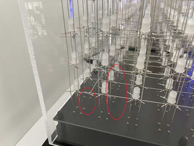
The Base
Overview
RGB LEDs have four leads, three for the cathodes and one for the anode (reversed if using a common cathode variant). The cube has 512 LEDs, each one individually addressable, controlling all the cathodes from a microcontroller individually would require too many wires and many IO ports to address each LED. Instead, we can rely on persistence of vision, allowing us to only light up a single level of the cube (64 LEDS) at a time by connecting all the cathodes in each column together. Which level is actively on, is controlled by supplying voltage to the anodes on the entire level, as all the anodes on a level are connected. Therefore, by controlling the 192 (64x3) cathode columns and the 8 anode levels, we can make the cube appear as desired by lighting up each vertical level in quick succession.
We can simplify controlling the cathodes by using a TLC5927 IC from Texas Instruments meant for controlling large LED sign displays. Each IC has a 16 bit shift register and data latches, allowing a serial data input, that is latched, allowing the control of current on each of its 16 ports. It’s purpose built for driving LEDs, and allows controlling the voltage across each LED by providing a single resistor (R-EXT) to the whole IC package, which controls the voltage sinked on each port. This is how we can avoid having a resistor attached to every single LED cathode in the cube. In the data sheet we can calculate in the chart provided which resistor value to use to get the desired mA on each cathode for the LEDs you are using.
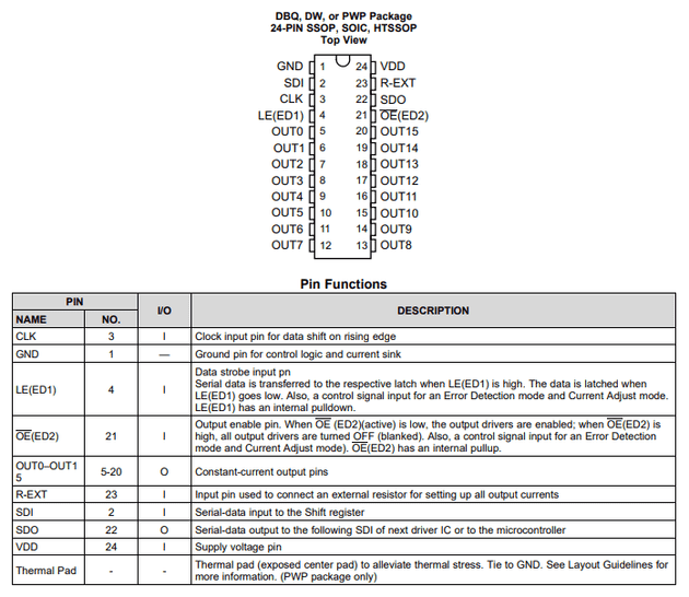
We need to control 192 cathodes, and each LED driver can control 16, so we need 12 of them. Instead of chaining all of them together in order to serially write data to them all, we will divide the cube into two chains, with 6 LED drivers on each chain, so that we can write out an entire levels data faster. Their control lines will be connected, but there data will be input from two separate signals.
On each chain of 6 drivers, the SDO of the first in the chain is connected to the SDI of the second and so on. We first drive the OE high in order to turn the LEDs off momentarily. We present one bit on the SDI of the first LED driver in each of the two chains, and pulse the clock, shifting it one position in the chain, repeat 95 more times to shift in the data for the whole chain. Then pulse the LE line to move the data from the shift registers to the output latches. We can drive OE low again, and the LEDs will turn back on. Leaving the OE low the whole time will cause the old and new data to coexist at the same time while the data is latching, which will cause the cube to show parts of both.
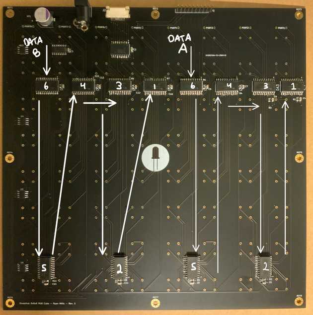
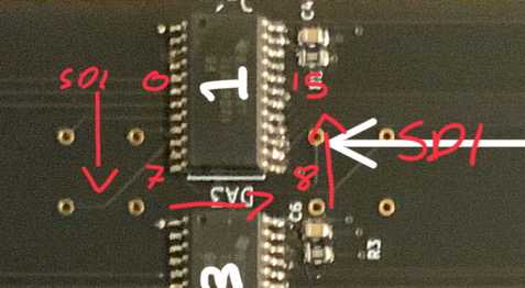
You will notice the shifting data into the drivers like this results in the data moving from the output 0 around to the output 15. Using Figure 10 as an example, as it references driver 1, the first bit placed into the chain will end up in output 15. In addition to this, logistically it is extremely difficult to place the drivers and route paths from each of the outputs to each of the LEDs in order, you can see this on the routes in Figure 9. So the driver outputs along the chain are mapped to the most convenient LED cathode. This results in needing a mapping of logical LED position to which position in the output buffer that LED needs to map to, so when a level’s cathode data is writen out, the buffer can sequentially write out its data.
{
  // Data A
  15, 14, 13, 12, 11, 10, 9, 8, 7, 6, 5, 4, 3, 2, 1, 0, // 1
  24, 25, 26, 27, 28, 29, 30, 31, 18, 17, 16, 21, 20, 19, 32, 23, // 2
  22, 35, 34, 33, 38, 37, 36, 41, 40, 39, 44, 43, 42, 47, 46, 45, // 3
  63, 62, 61, 60, 59, 58, 57, 56, 55, 54, 53, 52, 51, 50, 49, 48, // 4
  72, 73, 74, 75, 76, 77, 78, 79, 66, 65, 64, 69, 68, 67, 80, 71, // 5
  70, 83, 82, 81, 86, 85, 84, 89, 88, 87, 92, 91, 90, 95, 94, 93, // 6
  // Data B
  111, 110, 109, 108, 107, 106, 105, 104, 103, 102, 101, 100, 99, 98, 97, 96, // 1
  120, 121, 122, 123, 124, 125, 126, 127, 114, 113, 112, 117, 116, 115, 128, 119, // 2
  118, 131, 130, 129, 134, 133, 132, 137, 136, 135, 140, 139, 138, 143, 142, 141, // 3
  159, 158, 157, 156, 155, 154, 153, 152, 151, 150, 149, 148, 147, 146, 145, 144, // 4
  168, 169, 170, 171, 172, 173, 174, 175, 162, 161, 160, 165, 164, 163, 176, 167, // 5
  166, 179, 178, 177, 182, 181, 180, 185, 184, 183, 188, 187, 186, 191, 190, 189 // 6
};
Using this mapping, if we wanted to write to the very first LED, the LED in the very top right corner of Figure 9, its logical cathode indices would be [0, 1, 2](G, R, B), which when looked up in the table result in [ 15, 14, 13 ]. These indices would be where the data for 0, 1, 2 needs to be stored in the frame buffer for the level in order for a sequential write-out of the level data in the frame buffer to end up in the correct latches in the LED drivers.
Controlling each of the 8 anode levels is not possible from any microcontroller pins directly, as the appropriate current would not be provided from the microntroller itself. Each of the three colors in the LED are 20mA, so we would need 60mA * 64 = 3.84A theoritically if we were displaying solid white at full brightness. The Rext resistor value of 1KOhm chosen however allows each cathode run at 18.75mA, so slightly less total power needed.
To control driving the anodes of the levels, we can use P-Channel MOSFETs (FDS6975). We drive the gate of the transister low to allow the current from the main power source to flow to the anode levels, and drive it high to turn each level off.
To reduce the amount of data lines needed for the anodes, we can use a 3-to-8 line high speed decoder, SN74HC138DR to allow a binary representation to drive the MOSFETs.
This decoder inverts the outputs, so if we have anode control lines A, B, C (C is the most significant digit), driving the lines with 000 (LLL), will cause output 0 to be driven low, while the other lines are driven high. This is perfect for our use case with the P-channel MOSFETS, since we need to drive the selected anode level low in order to turn it on.
| Level To Turn On | Anode Ctrl C | Anode Ctrl B | Anode Ctrl A |
|---|---|---|---|
| 0 | 0 | 0 | 0 |
| 1 | 0 | 0 | 1 |
| 2 | 0 | 1 | 0 |
| 3 | 0 | 1 | 1 |
| 4 | 1 | 0 | 0 |
| 5 | 1 | 0 | 1 |
| 6 | 1 | 1 | 0 |
| 7 | 1 | 1 | 1 |
Essentially from the controller you output the binary number of the level you want to turn on, which is inverted in the decoder to select which of the 8 outputs is driven low, which leads to the gates of the MOSFETs, causing it to allow current from the main power source to flow to the level that should be on at that moment.
Therefore, we need a total of 8 signals from the microntroller to the cube to fully control it.
Control Lines
| Name | Purpose |
|---|---|
| LE | Latch the current data present in all the LED driver shift registers. |
| CLK | The clock controlling data into the LED driver ICs |
| OE | Output enable on the LED driver ICs. They output when low, and blank when high. |
| Data A | First data line for the LED drivers. |
| Data B | Second data line for the LED drivers. |
| Anode Control A | Least significant bit for selecting the anode level to turn on. |
| Anode Control B | Middle bit for selecting the anode level to turn on. |
| Anode Control C | Most significant bit for selecting the anode level to turn on. |
The ICs on the cube base operate on a 5v logic level, but the microntroller IOs are only 3.3v. To ensure reliable operation, a octal bus transiever is used, the HC74HC245, to convert between the two logic levels.
